- 您现在的位置:买卖IC网 > Sheet目录1992 > CY28378OXC (Silicon Laboratories Inc)IC CLOCK CK408/TITAN 845 48SSOP
CY28378
...................... Document #: 38-07519 Rev. ** Page 17 of 21
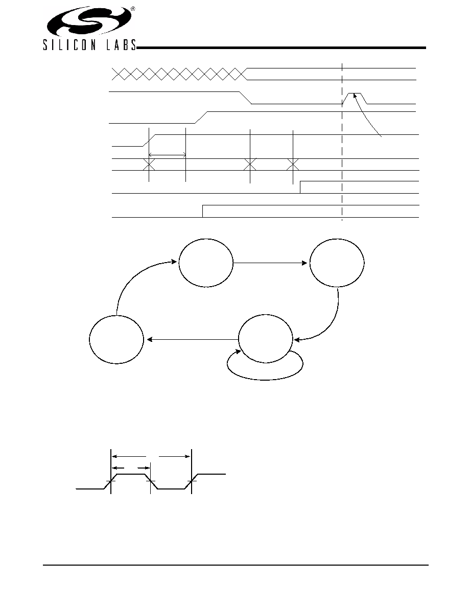
Switching Waveforms
Note:
6. Device is not affected, VTT_PWRGD# is ignored.
FS_A, FS_B
VTT_PWRGD#
PWRGD_VRM
VDD Clock Gen
Clock State
Clock Outputs
Clock VCO
0.2-0.3mS
Delay
State 0
State 2
State 3
Wait for
VTT_PWRGD#
Sample Sels
Off
On
State 1
Device is not affected,
VTT_PWRGD# is ignored
Figure 6. VTT_PWRGD# Timing Diagram[6]
VTT_PWRGD# = Low
Delay
>0.25mS
S1
Power Off
S0
VDDA = 2.0V
Sample
Inputs straps
S2
Normal
Operation
Wait for 1.146ms
Enable Outputs
S3
VTT_PWRGD# = toggle
VDDA = off
Figure 7. Clock Generator Power-up/Run State Diagram
Duty Cycle Timing
t1B
(Single-ended Output)
t1A
发布紧急采购,3分钟左右您将得到回复。
相关PDF资料
CY284108ZXC
IC CLOCK SERV CK410B 56TSSOP
CY28410OXC-2
IC CLOCK CK410 GRANTSDALE 56SSOP
CY28410OXC
IC CLOCK CK410 GRANTSDALE 56SSOP
CY28411ZXC
IC CLOCK CK410M ALVISO 56TSSOP
CY28442ZXC-2
IC CLOCK ALVISO PENTM 56TSSOP
CY28445LFXC-5
IC CLOCK CALISTOGA CK410M 68QFN
CY28446LFXC
IC CLOCK CALISTOGA CK410M 64QFN
CY28447LFXC
IC CLOCK CALISTOGA CK410M 72QFN
相关代理商/技术参数
CY28378OXCT
功能描述:时钟发生器及支持产品 Sys Clk Pentium 4 & Intel Brookdale 845 RoHS:否 制造商:Silicon Labs 类型:Clock Generators 最大输入频率:14.318 MHz 最大输出频率:166 MHz 输出端数量:16 占空比 - 最大:55 % 工作电源电压:3.3 V 工作电源电流:1 mA 最大工作温度:+ 85 C 安装风格:SMD/SMT 封装 / 箱体:QFN-56
CY28381
制造商:CYPRESS 制造商全称:Cypress Semiconductor 功能描述:High-Performance SiS645DX/648DX/650/651 Intel Pentium 4 Clock Synthesizer
CY28381OC
制造商:Rochester Electronics LLC 功能描述:- Bulk 制造商:Cypress Semiconductor 功能描述:
CY28381OCT
制造商:CYPRESS 制造商全称:Cypress Semiconductor 功能描述:High-Performance SiS645DX/648DX/650/651 Intel Pentium 4 Clock Synthesizer
CY28400
制造商:CYPRESS 制造商全称:Cypress Semiconductor 功能描述:100-MHz Differential Buffer for PCI Express and SATA
CY28400_05
制造商:CYPRESS 制造商全称:Cypress Semiconductor 功能描述:100-MHz Differential Buffer for PCI Express and SATA
CY28400-2
制造商:CYPRESS 制造商全称:Cypress Semiconductor 功能描述:100-MHz Differential Buffer for PCI Express and SATA
CY28400OC
功能描述:时钟缓冲器 100 MHz Diff Buffer PCI Express & SATA RoHS:否 制造商:Texas Instruments 输出端数量:5 最大输入频率:40 MHz 传播延迟(最大值): 电源电压-最大:3.45 V 电源电压-最小:2.375 V 最大功率耗散: 最大工作温度:+ 85 C 最小工作温度:- 40 C 封装 / 箱体:LLP-24 封装:Reel